On November 29, Prof. Lin Chen from Wuhan National Laboratory for Optoelectronics, Huazhong University of Science and Technology published new advances in NANO LETTERS. The paper is entitled High-resolution metalens imaging polarimetry.
As a fundamental property of light, polarization refers to the trajectory of the electric field vector. Measuring the Stokes vector of light enables exploring deeper information about an object, including its shape, texture, and birefringence/chirality. This capability is of significant interest in various scientific domains, particularly in the field of microscopic imaging. Traditional approaches for polarization imaging rely on bulk polarizing components and mechanical structures, leading to a large system volume and restricted temporal resolution.
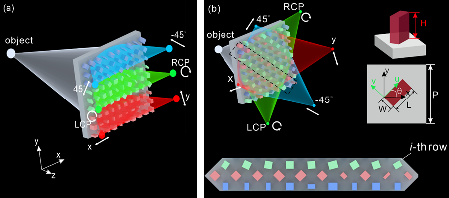
Metasurfaces have been proposed as a compact approach for imaging polarimeters. However, imaging polarimetry based on polarization-dependent metagratings and division of focal plane (DoFP) metalens for polarimetric imaging necessitate additional optical systems. In the DoFP method, the size of each metalens has to be sufficiently large to reduce the crosstalk between adjacent metalenses, so as to precisely restore the incident polarization. Consequently, the resolution of polarization imaging is constrained. More recently, a metalens imaging polarimetry segmented configuration is used, where the optical path between an object and discrete sub-metalens has to be almost equal, to reflect the polarization information of the object precisely (Figure 1a). This design method leads to a metalens polarimeter with a limited numerical aperture (NA), associated with a restricted imaging resolution of 5.8-fold wavelengths, and the NA below 0.1 experimentally.
Here, Lin Chen's team proposes an interleaved metalens configuration for polarization imaging, where three-row metasurface units within a group individually interact with three pairs of orthogonal polarization channels (Figure 1b). The optical paths between the object and adjacent three-row metasurfaces are nearly equal, allowing the construction of a metalens polarimeter with an unlimited numerical aperture (NA), beneficial for high-resolution polarization imaging.

Figure 1. Metalens imaging polarimeters. (a) Segmented metalens polarimeters. (b) Interleaved metalens polarimeters.
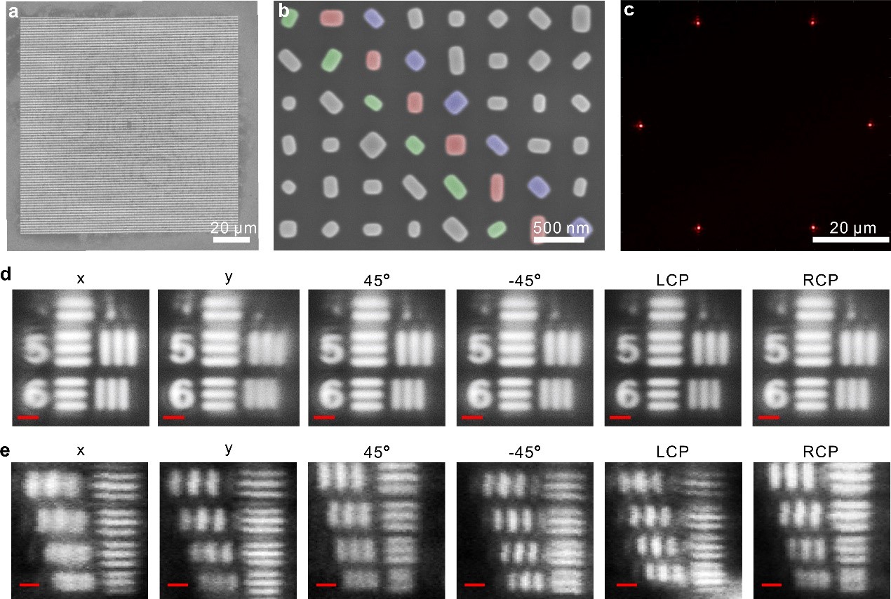
The metalens polarimeter fabricated by crystalline silicon nanostructures has an NA of 0.51 at 632.8 nm and achieves an imaging resolution of up to 1.2-fold wavelength (Figure 2a, b). Under the unpolarized light beam, one can observe the six focal spots for six polarization channels (Figure 2c). In the resolution-resolving experiment, the interleaved metalens polarimeters can clearly resolve the elements no. 5 and no. 6 from the 4th group (Figure 2d), and the elements no. 3 - no. 6 from the 7th group of the negative 1951 United States Air Force (USAF) resolution test chart at all six polarization channels (Figure 2e).

Figure 2. Fabrication and optical characterization of the interleaved metalens polarimeters. (a, b) SEM image. (c) Optical focusing image under the normal-incidence unpolarized light beam. (d) Images of elements no. 5 and no. 6 from the 4th group of USAF1951 resolution chart for six different polarization channels. (e) Images of elements no. 3-no. 6 from the 7th group of USAF1951 resolution chart for six different polarization channels.
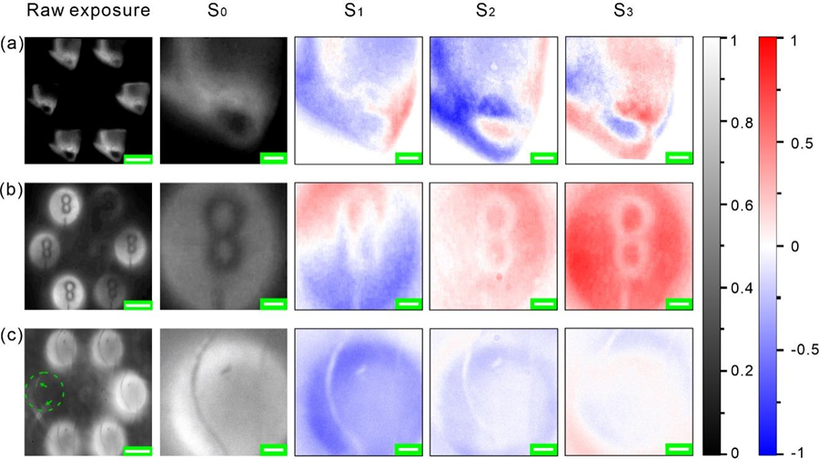
Polarimetric microscopy experiments demonstrate that metalens polarimeters can achieve high-resolution polarization imaging for various microscopic samples like quartz blocks (Figure 3a), plastic rulers (Figure 3b), and fish gill loading (Figure 3c) with high resolution. This study offers a promising solution for high-resolution metasurface polarization imaging with the potential for widespread applications, including remote sensing, astronomy, and biological detection.

Figure 3. Full-Stokes polarization imagery. (a) A crystal quartz. (b) A ruler. (c) A fish gill loading.
This work is supported by the National Key Research and Development Project of China (Grant No. 2021YFB2801903), the National Natural Science Foundation of China (Grant No. 12074137), and the Science, Technology and Innovation Commission of Shenzhen Municipality (Grant No. JCYJ20220530161010023). This paper is jointly collaborated with Mr. Zhaorui Huang, Dr. Junhao Li, Prof. Lin Chen from Wuhan National Laboratory for Optoelectronics, Huazhong University of Science and Technology, Mrs. Yaqin Zheng, Prof. Zhang-Kai Zhou from State Key Laboratory of Optoelectronic Materials and Technologies, School of Physics, Sun Yat-sen University, Prof. Yongzhi Cheng from School of Information Science and Engineering, Wuhan University of Science and Technology.
Link: https://pubs.acs.org/doi/epdf/10.1021/acs.nanolett.3c03258